The human eye can only see light at certain frequencies (called the visible spectrum), the lowest of which constitutes red light. Infrared light, which we can’t see, has an even lower frequency than red light. Researchers at the Indian Institute of Science (IISc) have now fabricated a device to increase or “up-convert” the frequency of short infrared light to the visible range.
Up-conversion of light has diverse applications, especially in defence and optical communications. In a first, the IISc team used a 2D material to design what they call a non-linear optical mirror stack to achieve this up-conversion, combined with widefield imaging capability. The stack consists of multilayered gallium selenide fixed to the top of a gold reflective surface, with a silicon dioxide layer sandwiched in between.
Traditional infrared imaging uses exotic low-energy bandgap semiconductors or micro-bolometer arrays, which usually pick up heat or absorption signatures from the object being studied. Infrared imaging and sensing is useful in diverse areas, from astronomy to chemistry. For example, when infrared light is passed through a gas, sensing how the light changes can help scientists tease out specific properties of the gas. Such sensing is not always possible using visible light.
However, existing infrared sensors are bulky and not very efficient. They are also export-restricted because of their utility in defence. There is, therefore, a critical need to develop indigenous and efficient devices.
The method used by the IISc team involves feeding an input infrared signal along with a pump beam onto the mirror stack. The nonlinear optical properties of the material constituting the stack result in a mixing of the frequencies, leading to an output beam of increased (up-converted) frequency, but with the rest of the properties intact. Using this method, they were able to up-convert infrared light of wavelength around 1550 nm to 622 nm visible light. The output light wave can be detected using traditional silicon-based cameras.
“This process is coherent – the properties of the input beam are preserved at the output. This means that if one imprints a particular pattern in the input infrared frequency, it automatically gets transferred to the new output frequency,” explains Varun Raghunathan, Associate Professor in the Department of Electrical Communication Engineering (ECE) and corresponding author of the study published in Laser & Photonics Reviews.

The advantage of using gallium selenide, he adds, is its high optical nonlinearity, which means that a single photon of infrared light and a single photon of the pump beam could combine to give a single photon of light with up-converted frequency. The team was able to achieve the up-conversion even with a thin layer of gallium selenide measuring just 45 nm. The small size makes it more cost-effective than traditional devices that use centimetre-sized crystals. Its performance was also found to be comparable to current state-of-the-art up-conversion imaging systems.
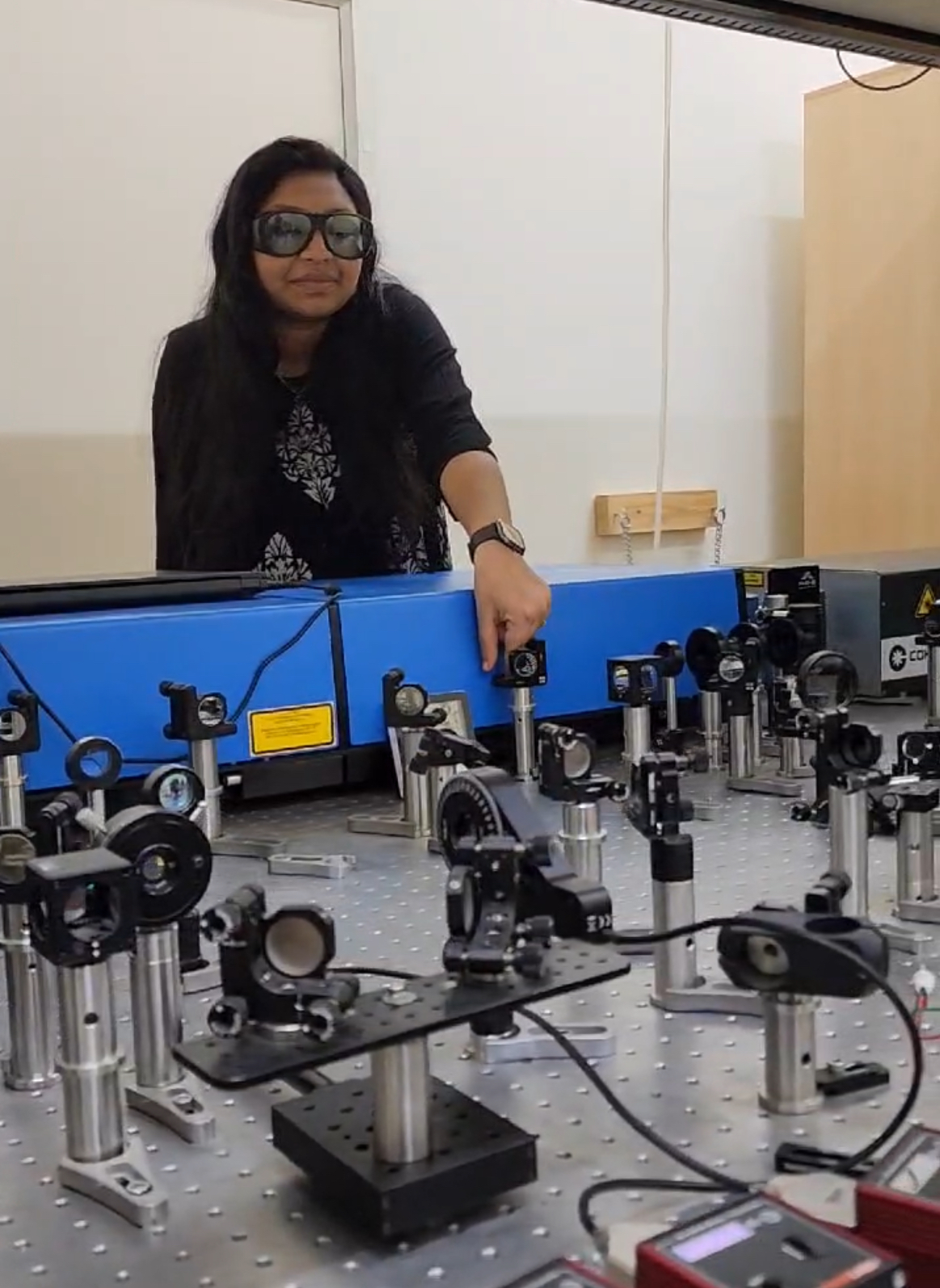
Jyothsna K Manattayil, PhD student at ECE and first author, explains that they used a particle swarm optimisation algorithm to speed up the calculation of the right thickness of layers needed. Depending on the thickness, the wavelengths that can pass through gallium selenide and get up-converted will vary. This means that the material thickness needs to be tweaked depending on the application. “In our experiments, we have used infrared light of 1550 nm and a pump beam of 1040 nm. But that doesn’t mean that it won’t work for other wavelengths,” she says. “We saw that the performance didn’t drop for a wide range of infrared wavelengths, from 1400 nm to 1700 nm.”
Going forward, the researchers plan to extend their work to up-convert light of longer wavelengths. They are also trying to improve the efficiency of the device by exploring other stack geometries.
“There is a lot of interest worldwide in doing infrared imaging without using infrared sensors. Our work could be a gamechanger for those applications,” says Raghunathan.
