Pavan Nukala’s lab delves deep into how nanomaterials behave

A big portion of our lives is centralised around tiny devices: computer chips, LEDs, batteries, CDs, and so on. Materials at the nanometric scale – 1 millionth of a millimetre – show exotic phenomena that can be used to make our lives easier. How does one study something so small?
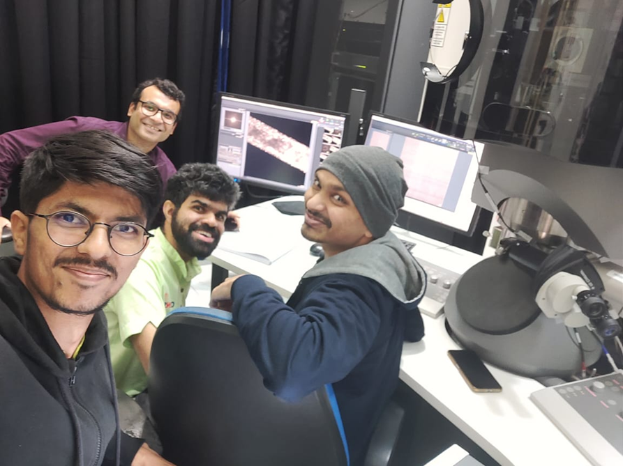
In the lab led by Pavan Nukala at the Centre for Nano Science and Engineering (CeNSE), seeing is understanding. “By visually observing the materials in action using electron microscopy, we are able to understand something new. This was my philosophy when I joined IISc and started my research group,” explains Pavan, Associate Professor at CeNSE.
When Pavan was in his fourth year of Bachelor’s studies in Metallurgy and Materials Engineering at IIT Madras, he did not know what to do next. He decided to do a project on photonics – the study of light-matter interactions. He was so intrigued that he went on to apply for a PhD in it.
Pavan joined as a graduate student at UPenn under faculty member Ritesh Agarwal, who also worked on photonics. “But I came from a materials science background, so we settled on working on phase change memory (PCM) materials,” he recalls. “This is the technology employed in making rewritable memory devices.”
Phases and memories
Many materials have two phases within their solid state: amorphous and crystalline. The amorphous phase arises when molecules are present in a random, disordered manner, whereas a crystalline material has molecules arranged in a repeating pattern. A rewritable CD works by using a thin, continuous layer of a material – typically a chalcogenide alloy. This layer contains billions of tiny sites that can individually change their phase. A CD reader will read a crystalline site as 1 and an amorphous site as 0, thus storing binary data. To convert a crystalline material into its amorphous state, we need to melt it briefly into its liquid form and then quickly cool it, a technique called melt quenching. The heat is supplied through a laser or electrical pulses.
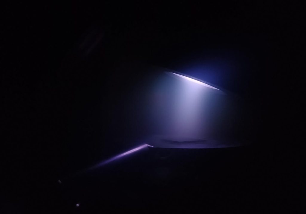
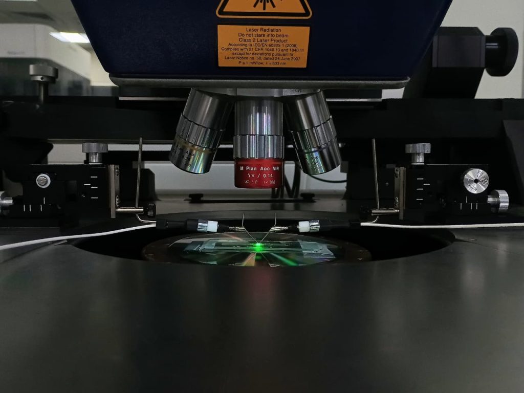
This concept fascinated Pavan, and he wanted to understand what exactly happens to the material during its phase change. One way to visualise molecules inside the material is via an electron microscope, which employs electrons instead of light to image objects. “Using an electron microscope, you can even image atoms. Our plan was to observe a nanomaterial while it was given an electrical impulse so that we could understand these phenomena atomistically.” This procedure, known as in situ electron microscopy, is a common technique used in Pavan’s lab group today.
“At that time, in situ microscopy was not a big thing. People were getting into it, but they were not happy with how the energetic electrons could potentially change the material itself. We were among the first to observe the phenomena of phase change using an electron microscope,” recalls Pavan. “We had to build our own instruments for this. We did it, and we saw something beautiful.”
It turned out that electrical pulses create dislocations or defects within the material structure. These defects can move freely and interact with moving electrons. This way, an electric current can also carry these defects.
“Now, if we cause some constrictions on the materials, we can create a jam in the flow of defects. Thus, defects accumulate. Once you have enough jams in the traffic, the order breaks down and the crystalline material is amorphised,” Pavan explains. This method offered a much more efficient way than melt quenching.
On thin films
Pavan’s interest in electron microscopy did not end there. “What fascinated me as a grad student were these atomic scale images of that were coming out. There were many papers where people would showed columns of atoms. Those were the early days of aberration corrected, directly interpretable, high-resolution electron microscopy.”
Those images were of complex oxides. Some compounds of such oxides – like copper oxide-based materials – showed high-temperature superconductivity. A metal like gold becomes a superconductor at a few milli-Kelvins (K), while these compounds did so at around 100 K.
“The Holy Grail of materials science around the 1980s was to push this limit upwards so we can have superconductors at room temperature,” explains Pavan. “This was never achieved, but as a result, people got used to growing thin films of single crystalline oxides, one atomic layer by another on a substrate.” Thin films – about 10,000 thinner than a strand of hair – have fewer defects.
Apart from potential superconductivity, oxides have very rich physics. Pavan decided to join a research group in France that works on them. “I became their local Transmission Electron Microscope (TEM) guy, and I got to work with a lot of images of atoms.”
These images were not just for show; they answered several questions that had popped up about these oxides, ferroelectricity in hafnia based materials. A ferroelectric material has an inherent electric dipole that can be reversed. Pavan’s research using in-situ electron microscopy, now at atomic scale resolution, showed that moving positively-charged oxygen vacancies and their motion was the mechanism that drove this ferroelectricity.
“Once again, by looking at the materials in action, we were able to understand how and why the material works. This was the basic idea of our group when I joined CeNSE in 2020. First, we understand the materials. Then, we can use it as feedback and construct useful devices,” he explains.
Shaking up the material world
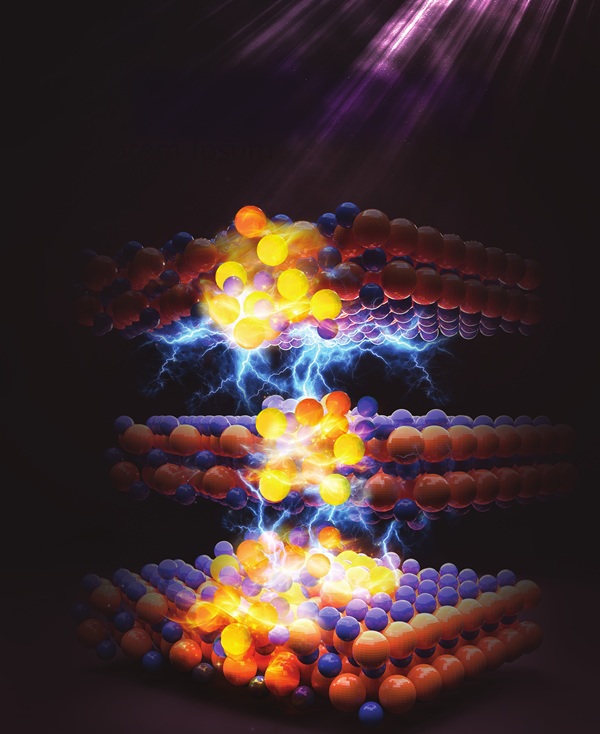
Recently, Pavan’s group was working in collaboration with his former PhD advisor on Indium Selenide. “Indium Selenide had two-dimensional layers stacked on top of each other and is also ferroelectric. If you apply a current across a nanowire and you keep on increasing the potential difference, at some point the current vanishes,” says Pavan. This was completely unexpected. Why would a conductor suddenly become an insulator?
When the team looked at the nanowire under the TEM, they realised that if the electric field is large enough and is lateral to the ferroelectric dipole moment, the entire nanowire amorphises. “Amorphous solids are poor conductors,” explains Pavan. “We immediately knew that this was interesting as we had never seen such amorphisation.”
Further investigation allowed the team to understand the reason. Every ferroelectric material is also piezoelectric – an electric field causes mechanical strain in the material. “This causes shocks in the crystalline structure that propagate like earthquakes in a city. We knew this happens for ordinary (3D) ferroelectric materials, but they recover after the shock wave subsides because of the strong bonds. However, if your material is two-dimensional, it is not able to withstand the shock, and the well-ordered structure breaks down, amorphising the material,” explains Pavan. This is again a very promising method for PCMs, as it is significantly more efficient than melt quenching in terms of power consumption.
“Further, the noise that we observed from the TEM images was similar to that of the brain under an MRI scan. Naturally, we started to think: was this noise to be discarded, or does it contain some hidden information? This is currently pushing us in the direction of noise based (neuromorphic) computing approaches,” remarks Pavan.
What Pavan enjoys most about research in materials science is the fact that new, ingenious ideas and questions pop up every day. He compares this to Huygen’s principle of propagation of waves like light or electrons. At each point on the wavefront, wavelets are created, which spread outward and generate even more wavelets. This way, the wave propagates. “The first wavelet is made by asking the right question, and the second one by doing experiments and generating models, which ends up generating more questions or wavelets. This is essentially research,” he explains. “This process is addictive, and I am proud to say that I am addicted.”