20 years after its discovery, scientists are still trying to unleash the full potential of this unique material
Arindam Ghosh first learned about graphene in 2004 when he was doing his postdoc at Cambridge University. He was listening to a talk by University of Manchester physicist Konstantin Novoselov describing a paper that the latter was about to publish on the discovery of this new “wonder” material. “I was one of the people who interacted with him at that time. It was a captivating talk, and we all anticipated the paper’s publication,” Arindam recalls.
The Science paper, which came out in October 2004, described Konstantin and his advisor Andre Geim’s success at isolating a single sheet of graphene for the first time. It was heralded as a huge breakthrough, leading to the duo winning the Nobel Prize a few years later.
“When I returned to India in 2005, I realised that it was a great time to work on graphene,” recalls Arindam, now Professor at the Department of Physics, IISc. “Unlike other cutting-edge materials, graphene research didn’t require access to high-quality facilities to obtain the material, therefore creating a fantastic equalising impact, whether you were at MIT, Harvard, or elsewhere.”
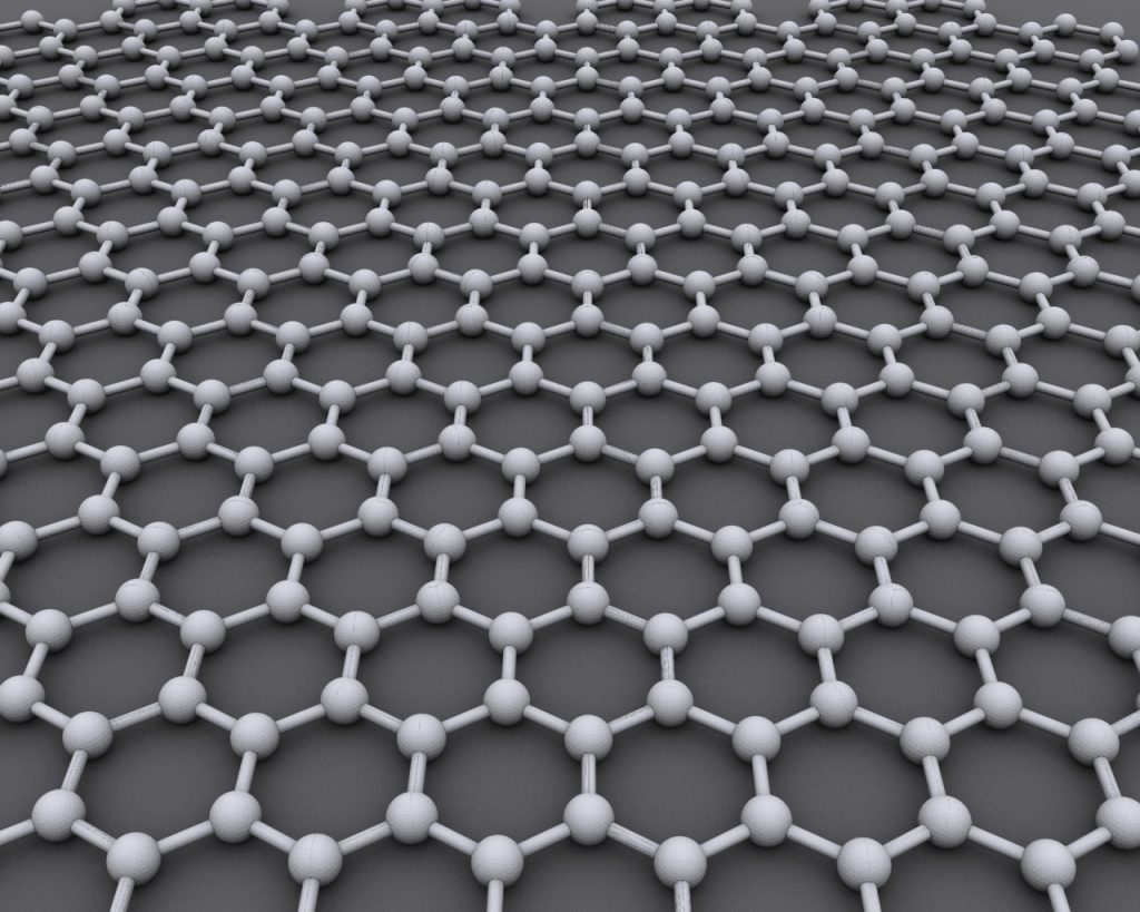
This year marks the 20th anniversary of the discovery of graphene, a material that scientists believe can transform our world – from revolutionising electronics to developing next-generation materials. It isn’t just incredibly thin; it’s the ultimate microscopic building block. Imagine a single layer of carbon atoms arranged in a honeycomb pattern, a million times thinner than paper but with strength rivalling chain mail. This unique combination, along with its exceptional electrical conductivity and unmatched heat resistance, has fascinated the scientific community since its discovery.
At IISc, researchers like Arindam are not only trying to understand graphene’s unique properties but also tackling the hurdles that need to be overcome for its large-scale integration into future technologies.
“The discovery of graphene was the result of efforts spanning many years, dating back to 1947 when theorists predicted its existing properties,” Arindam explains. Before 2004, researchers tried immersing graphite in extreme environments – for example, dunking it in liquid helium – to separate graphene layers but had limited success. The Manchester team hit upon a clever solution. They realised that Scanning Tunneling Microscopy experts often used Scotch tape to obtain clean graphite surfaces. So, they repeatedly exfoliated graphite with Scotch tape and then transferred it onto a glass or silicon dioxide (SiO2) wafer. This simple yet ingenious method and their understanding of graphite properties ultimately led to the successful isolation of single-layer graphene. Later, they found a simpler method – pressing graphite onto a SiO2 wafer with Scotch tape left behind single layers.
Graphene has become significant not just because of its exceptional properties, but also the promise it offers for future applications, whether in electronics, polymers or lightweight structures for the aviation industry. “Additionally, the discovery of graphene led to extensive research on other 2D materials, essentially starting a new field and leading to new physics and technology demonstrations,” Arindam adds.
Delving deep
Around the time Arindam returned to India, IISc acquired a state-of-the-art lithography facility. Aided by a helium-3 cooling system and a team of students who could carry out exfoliation of graphite, Arindam began delving into the fundamental properties of graphene.
“Our first goal was to investigate noise,” Arindam recollects. Although graphene was being touted as the “next silicon”, scientists soon realised that graphene couldn’t become a standard electronic component due to its zero band gap. However, it had potential for other electronic applications. “My group specialises in electronics,” says Arindam, “and we were interested in noise measurements. So, we started a project to understand if graphene is a noisy conductor – which could limit its electronic applications – and what information we could glean from noise measurements.”
Graphene is typically a single crystal with minimal defects so it should ideally be noise-free. So where does the noise come from? It comes from two external sources: the contacts and the substrate. Additionally, the lithography process exposes the surface to chemicals which also contribute to noise. These three sources of noise needed to be addressed. “Over the next two years, we perfected the technique of making better-quality graphene devices. Eventually, we achieved graphene with the lowest noise ever in 2020 after about 10-12 years of continuous work,” Arindam explains.
In 2012, his lab made another leap forward. For the first time, they tried combining graphene with molybdenum disulphide, another 2D material, and found that the hybrid material was superior to both in detecting and responding to light. It opened up new possibilities in materials science and device engineering.
Graphene’s potential is not limited to electronics. In composite materials, graphene can help enhance gas resistance or tensile strength. It can bind to biological species effectively, opening up possibilities for biosensing. Many researchers are exploring its use in early disease detection – by attaching antibodies to graphene surfaces and detecting antigens from swabs or blood samples.
“While graphene boasts immense potential, translating that potential into real-world applications presents challenges,” acknowledges Arindam.
Scaling up
If graphene needs to go truly commercial, it requires large, wafer-scale production facilities and techniques. This is where processes like Chemical Vapour Deposition (CVD) come in, says Srinivasan Raghavan, Professor and Chair of the Centre for Nano Science and Engineering (CeNSE), IISc. His lab not only focuses on large-scale fabrication of graphene, but also growing other 2D materials like boron nitride and molybdenum sulphide (MoS2) over large areas. “To make electronics, one needs the whole palette metal (graphene), semiconductor (MoS2) and insulator (boron nitride),” he explains.
In 2009, nanoscience researcher Rodney Ruoff’s team published a landmark study in Science showing how graphene can be deposited on large copper sheets. “Around that time, our team primarily worked with gallium nitride (GaN). Arindam contacted us, knowing our expertise in CVD, and asked if we could grow graphene. At that point, I hadn’t given much attention to graphene. However, I decided to take on the challenge and asked my student, Tanushree Chowdhury, to tackle it,” Srinivasan recalls.
Tanushree and the team placed a sheet of copper inside a CVD reactor that they were using to fabricate GaN and inserted a pipe containing methane gas into it. They immediately observed the characteristic Raman spectroscopy peaks of graphene. “Remarkably, on our very first attempt, we successfully grew graphene. I was pleasantly shocked by it. As a postdoc, it had taken me a year just to grow one layer of GaN,” Srinivasan says. He and Arindam co-published a paper with both their students as co-first authors. “This was the first paper from India on large-area graphene.”
Bolstered by this attempt, Srinivasan thought that growing graphene on a large scale would be quite easy. “I felt somewhat overconfident,” he admits. “Later on, I was proved wrong. We realised that typically when graphene grows over large areas, it is not a single crystal; it’s a polycrystal.” A former student of Srinivasan, Krishna Balasubramanian, now a faculty member at IIT Delhi, showed that graphene nucleates and grows as flakes on copper foil. They merge and form grain boundaries and defects called triple junctions.
“Consistent layers are essential when considering graphene or other 2D materials for electronic device applications that require large-area production. In our lab, we can coat a 1-foot by 3-foot sheet of copper with predominantly monolayer graphene by tweaking conditions to minimise bilayer patches,” he says.
Because graphene grows layer by layer, large-scale fabrication also offers scientists an opportunity to understand the mechanism of atomic layer growth, Srinivasan says. “This gives us more insight into understanding and improving crystal growth.”
Despite the challenges in growing large-scale graphene, Srinivasan and others are encouraged by the sheer scope of practical applications.
For example, even defect-filled large-area graphene can be used for packaging. “Packaging applications can be divided into two main categories. One involves high-tech, lightweight, flexible electronics packaging, where graphene provides an impermeable, EMI-shielding layer,” explains Srinivasan. “The other category focuses on eco-friendly packaging solutions. For instance, paper and biodegradable plastics are permeable to water. Can a graphene layer make them impermeable and robust enough?” Graphene-coated materials could replace hard-to-recycle materials like aluminium-coated plastics or Tetra packs because they are more environment-friendly.
Srinivasan has also collaborated with Praveen Ramamurthy, Professor in the Department of Materials Engineering, to show that graphene can be used for packaging solar cells. “When solar cells are packaged with graphene-containing polymer hybrids, the lifetime is much longer,” he adds.
Arindam and Srinivasan believe that the time is ripe to prioritise such applications. “Moving towards real-world applications and commercial viability,” Arindam says, “is critical for the future of graphene.”


