Techniques that allow etching of patterns for fabricating practically useful devices
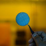
In a room filled with orange light, a researcher fully covered from head to toe with a face mask, bunny gown, gloves and shoe covers carefully holds a black round disk. This is a typical scene at the cleanroom of the National Nano-fabrication Centre (NNFC) at the Centre for Nano Science and Engineering (CeNSE), where researchers fabricate devices with parts smaller than the width of a human hair. The protective gear is essential because even the smallest speck of dust or a single strand of hair can disrupt the microscopic patterns. The distinctive orange lighting comes from special sodium vapour lamps that do not emit ultraviolet light that could interfere with the delicate manufacturing process. The black round disc is a silicon wafer on which patterns are etched, a process called micropatterning.
Micropatterning can be done using photolithography, which uses visible light and a design mask to project micrometer-sized patterns onto a light-sensitive material. The projected patterns are then specifically removed, in a process called etching, to create precise features.
Photolithography emerged in the 1950s, when the semiconductor industry was in its infancy. Engineers discovered that they could use light to “print” microscopic patterns on silicon, much like developing a photograph. This breakthrough enabled computer engineers to fabricate complex integrated circuits onto increasingly smaller chips, paving the way for modern computing.
Other types of lithography, such as X-ray lithography and e-beam lithography offer different ways to create patterns at smaller scales. For example, e-beam lithography uses a focused electron beam to directly write tiny patterns onto a surface coated with a special material, offering high precision but at a lower speed and higher cost.
Photolithography is not useful just for making computing devices. It is also required for designing microelectromechanical systems (MEMS) that find use in diverse areas.
Gayathri Pillai, Assistant Professor at CeNSE, uses photolithography to fabricate MEMS and NEMS (nanoelectromechanical systems), which can convert electrical to mechanical energy and vice versa. The patterns etched on them using light may stretch from a few hundred nanometres to millimeters.
To construct these devices, researchers first create a 3D design mask of the patterns. Then, a thin light-sensitive coating called photoresist is applied on the material to be used for micropatterning. Next, light passes through the design mask and hits the areas of the material not covered by the mask. If a positive photoresist is used, the areas exposed to light can be washed away by dipping the material in a developer solution for a few seconds, leaving behind the design on the surface.
“Every second matters during the development step. It heavily depends on the surrounding conditions such as moisture, due to which the sample may become over-developed or underdeveloped,” says Linet Thomas, a PhD student in Gayathri’s lab. Since the patterns are so small, even tiny dust particles and strands of hair may cause defects. Dust particles may also obstruct the path of light while the patterns are being etched. This is why the process is carried out in a cleanroom.
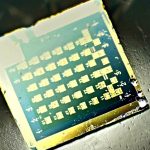
Linet is currently in the process of constructing a Piezoelectric Micromachined Ultrasound Transducer (PMUT) device using photolithography. Piezoelectrics are materials that can convert electrical energy into mechanical energy and vice versa. PMUTs can be used to generate and detect ultrasound waves used in medical imaging, like pregnancy scans, and in other applications such as non-destructive testing, range finding and fingerprint scans.
These piezoelectric materials can be grown or deposited over a specific substrate to make them vibrate, producing ultrasound waves of a wide range of frequencies. Cantilevers are beam-like structures supported at one end, and free to move on the other. In a typical microfabrication process for a solid state device, patterns are only defined from the top side. “To fabricate a cantilever that needs space to move, material is etched from the bottom as well,” explains Gayathri. The alignment between the top and bottom etching must be precise down to the micrometer scale – like digging a tunnel through a mountain from both ends such that the two paths perfectly meet in the middle.
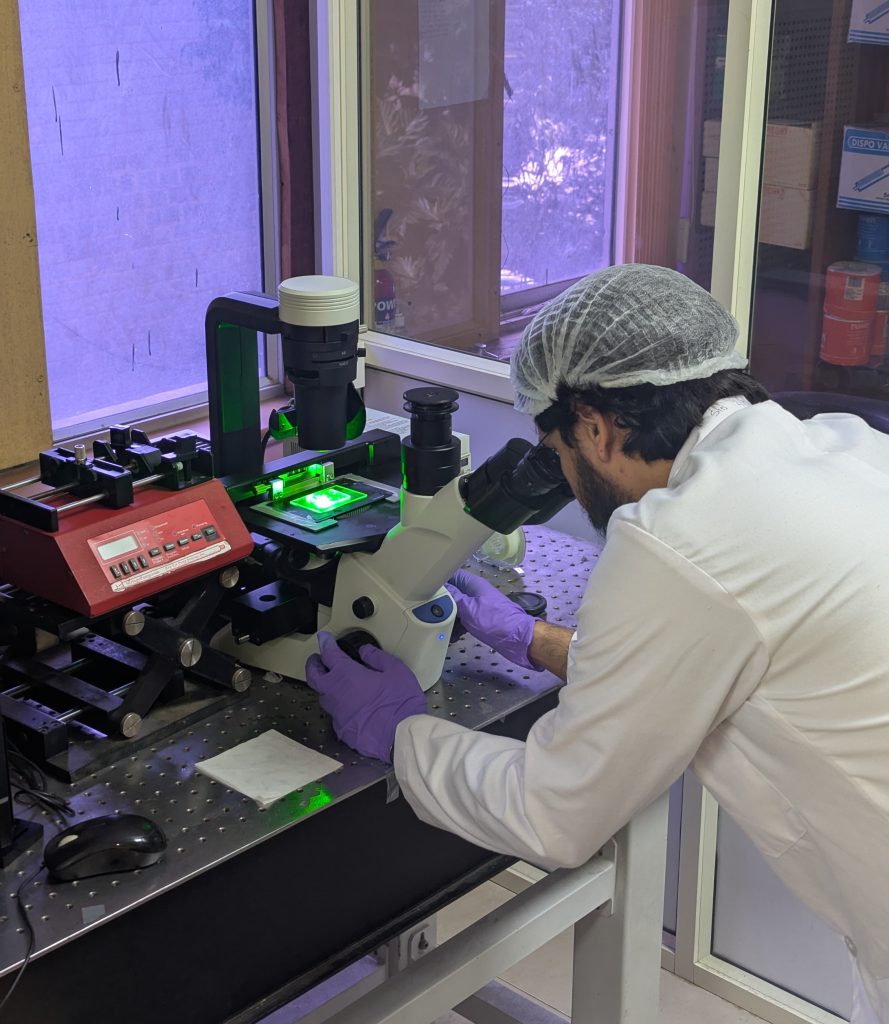
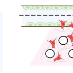
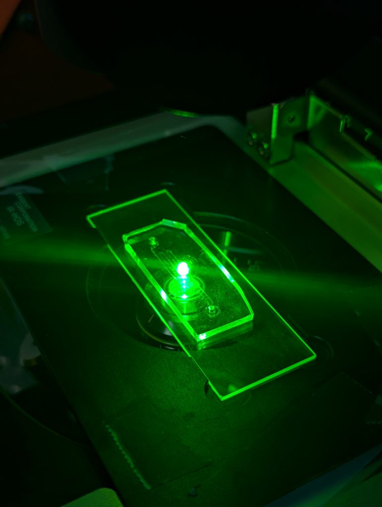
Micropatterning is also used to fabricate microfluidic devices in the lab of Saptarshi Basu, Professor at the Department of Mechanical Engineering. His lab uses these devices to build organ-on-chip models, which contain a small piece of material etched with tiny channels and spaces that can house cells from an actual organ. In the lab, cells are grown on these channels, just like how they grow inside the body. The chip can also simulate the organ’s function by pumping fluids or air through the channels, much like how blood flows through blood vessels, or by providing nutrients to the cells like our body does. For example, a heart-on-a-chip can even make the heart cells beat artificially. Saptarshi’s group places bacterial cells in such microchannels and mimics their movement through arteries in our body to study how they react to mechanical stress during the flow.
While lithography is quite useful in fabricating such devices, it has its own challenges. For one, it can generate a lot of material waste. Second, even in a controlled cleanroom environment, factors such as humidity and the number of people present may lead to different developing times. This reduces the reproducibility of photolithography – crucial for industrial applications. “It is a very user-dependent skill since the development process only takes a couple of seconds sometimes,” explains Gayathri. It is also expensive and difficult to maintain cleanrooms necessary for photolithography.
To overcome some of these problems, Saptarshi’s group is working on a method called 3D inkjet printing. “Similar to how the Ajanta and Ellora temples were constructed, in lithography, material is etched away from the top [to bottom]. However, 3D inkjet printing is a bottom-up approach,” he explains. This technology can be used to build microbioreactors and microfluidics-based point-of-care diagnostic devices. In this method, material is added in the form of tiny droplets layer by layer from the bottom to the top.
Since this method does not require a cleanroom, costs are lower. Still, 3D inkjet printing cannot achieve the same level of detail as photolithography. This limitation stems from the relatively large size of the ink droplets used in 3D printing, typically ranging from 10 to 50 micrometers. Even with advanced technology, the inherent properties of liquids, such as surface tension and spreading, prevent the creation of features smaller than a micrometer.
There are also other advances in lithography such as Extreme Ultraviolet lithography systems that can now create patterns just 3 nanometers wide.“Development of alternative methods of micropatterning such as 3D inkjet printing without the need for a cleanroom will reduce costs and contribute to ‘Make in India,’” Saptarshi adds.

